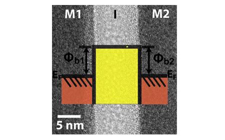
[tooltip text=”Tooltip Text”]
August 9, 2013
9:00am – 5:00pm
Vivere Hotel, Alabang
Fee: Php 5,500.00 / person plus 12% VAT
NOTE: Student Rate: P2,000.00 per person.
(please present a valid school ID upon registration)
- Early Registration Payment: Ten-Percent (10%) Discount if PAID thirty (30) days before the training date
- Group Discount: Five-Percent (5%) on Three (3) or More Participants
[tabs slidertype=”left tabs”]
[tabcontainer]
[tabtext] About [/tabtext]
[tabtext] Course Outline [/tabtext]
[tabtext] Facilitator [/tabtext]
[tabtext] Bank Details [/tabtext]
[/tabcontainer]
[tabcontent]
[tab]
Synopsis:
The dawn of tunnel diodes, commonly attributed to Leo Esaki in the late 1950’s, predates much of the innovation and infrastructure investment into CMOS technology. But, the lack of a mass production process and inability to monolithically integrate these devices into complex circuits paved the way for the CMOS juggernaut seen today.
However, the unique negative differential resistance (NDR) systemic to all tunnel diodes provides a pathway to exploit new hybrid-CMOS circuit topologies with compact latches and reduced power consumption that could mitigate some of the bottlenecks perceived for scaled CMOS. A new paradigm of computing is possible, capitalizing upon transistor/tunnel diode integration if a viable Si-based tunnel diode could be developed. This talk will explore these opportunities.
Si-based resonant tunnel diodes (RTD) function via intraband tunneling through a confined quantum well state formed by double heterobarrier cladding. However, finding a suitable well and barrier material that are epitaxially compatible is a heated materials science topic. Si and SiGe provide a large valence band offset, but due to the large effective mass of holes, the valence band state becomes too diffuse to permit significant room temperature NDR behavior. Si/SiGe can provide a modest conduction band offset if a virtual SiGe substrate is used for strain engineering. Other barrier layers, including various oxides, are actively being pursued as a replacement, but these present a materials science compatibility problem that requires greater study.
By trading one materials science dilemma with another, studies of Si-based interband tunnel diodes were re-visited in the late 1990’s, but via an epitaxial platform instead of the Esaki-era alloy process. The key hindrance to this approach is dopant diffusion and segregation that prevents degenerate doping across a narrow p-n junction. This team pursued the usage of ?-doping and low temperature molecular beam epitaxy (LT-MBE) to suppress the dopant redistribution. If the growth and processing conditions are optimized, the ?-doping layers can create quantum wells leading to a Si-based resonant interband tunneling diode (RITD) configuration.
This talk will provide a background on Si-based tunnel diode devices and circuits and summarize the results of Si-based RITD device optimization, their monolithic integration with Si-based transistors and present a range of circuit prototyping. Recent developments to technology transfer this technology from molecular beam epitaxy (MBE) to standard CMOS chemical vapor deposition (CVD) will be highlighted. The extension of NDR to ultra-low voltage memory will also be discussed.
Objectives of the Course:
- To understand the challenges of continued MOSFET scaling beyond the 22nm node
- To get a brief overview of the options available to industry and their pros and cons
- Then to more fully explore the one thrust (my own) related to “negative differential
resistance”- Motivation of NDR circuits
- NDR device physics
- Materials science challenges of NDR devices
- Examples of best performers
- Overview of NDR circuits empowered (memory, communications & logic)
[/tab]
[tab]
Course Outline
Negative Differential Resistance Devices and Circuits
- Introduction, Background and Motivation
- NDR Device Model
- Large Signal Mode
- Small Signal Mode
- NDR Device Performance Metrics
- DC Performance Metrics
- AC Performance Metrics
- Basic Physics of Quantum Mechanic Tunneling
- Tunneling through a Barrier
- Interband versus Intraband Tunnel Diodes
- Valley Current Components
- Phonon Participation in Interband Tunnel Diodes
- Diode Thermal Diffusion Current
- Total Tunnel Diode Current
- Basic NDR Devices
- Esaki Diodes
- Resonant Tunneling Diodes
- Resonant Interband Tunneling Diodes
- Three Terminal NDR Devices
- Materials and Epitaxial Growth Issues
- Band Offsets of Heterostructures
- Influence of Interface Roughness
- Influence of Doping Profile
- Summary of NDR Devices
- Esaki-like Interband Tunnel Diodes
- III-V RTDS
- III-V RITDs
- Unique Challenges of Si-Based NDR Devices
- Organic NDR Devices
- Radiation Immunity
- NDR Circuits
- Introduction – Speed, Power, Device Count Tradeoffs
- Integration of NDR devices with Transistor Technologies
- Logic Applications
- NDR Memory Applications
- NDR Mixed-Signal Applications
- Oscillators
- Conclusions and Future Outlook
[/tab]
[tab]
Paul R. Berger
Department of Electrical Engineering and Department of Physics
The Ohio State University, Columbus, OH 43210
Paul R. Berger is a Professor in Electrical & Computer Engineering at Ohio State University and Physics (by Courtesy). He is the Founder of the Nanoscale Patterning Laboratory. He received the B.S.E. in engineering physics, and the M.S.E. and Ph.D. (1990) in electrical engineering, respectively, all from the University of Michigan, Ann Arbor.
Currently, Dr. Berger is actively working on conjugated polymer-based optoelectronic and electronic devices; molecular electronics; Si/SiGe nanoelectronic devices and fabrication processes; Si-based resonant interband tunneling diodes and quantum functional circuitry; and semiconductor materials, fabrication and growth.
Formerly, he worked at Bell Laboratories, Murray Hill, NJ (1990-’92) and taught at the University of Delaware in Electrical and Computer Engineering (1992-2000). In 1999, Prof. Berger took a sabbatical leave while working first at the Max-Planck Institute for Polymer Research, Mainz, Germany while supported by Prof. Dr. Gerhard Wegner and then moved on to Cambridge Display Technology, Ltd., Cambridge, United Kingdom working under Dr. Jeremy Burroughes. In 2008, Prof. Berger spent an extended sabbatical leave at IMEC (Interuniversity Microelectronics Center) in Leuven, Belgium while appointed as a Visiting Professor in the Department of Metallurgy and Materials Engineering, Katholieke Universiteit Leuven, Belgium.
He has authored ~100 articles, 5 book sections and been issued 16 patents with 4 more pending. Some notable recognitions for Dr. Berger were an NSF CAREER Award (1996), a DARPA ULTRA Sustained Excellence Award (1998), a Lumley Research Award (2006, 2011), and a Faculty Diversity Excellence Award (2009). He has been on the Program and Advisory Committees of numerous conferences, including the IEDM, ISDRS meetings. He currently is the Chair of the Columbus IEEE EDS/LEOS Chapter and Faculty Advisor to Ohio State’s IEEE Student Chapters. He is a Fellow and Distinguished Lecturer of IEEE EDS and a Senior member of Optical Society of America.
[/tab]
[tab]
BANCO DE ORO (BDO)
Account Name:
Aguila Group Companies (AGC) Development Corporation
Account Number:
00 543 801 3291
Bank Address:
Alfaro-Salcedo Village Branch, PCCI Bldg., 118 Alfaro St., Salcedo Village, Makati City 1227, Philippines
Swift Code:
BNORPHMM
[/tab]
[/tabcontent]
[/tabs]


+ There are no comments
Add yours